
Dry Environment - The Role of Particulation in Semiconductor
Dry Environment - The Role of Particulation in Semiconductor
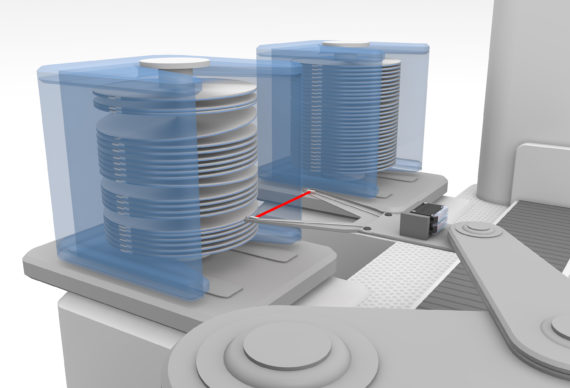
Particulation in terms of Semiconductor is a phenomenon where materials shed micro particulate while rubbing in contact with other materials. The shed particles, often in the 10 µm range or smaller can be a source of contamination leading to issues caused by abrasion in the processing of the wafer. Applications that are most concerned with particulation or the generation of particles are often associated with wafer mobility or wafer storage.
There is not a tremendous amount of information available in terms of particulation generated with respect to plastics, however testing has shown that crystalline and semi crystalline materials resist the generation of particles more so than amorphous materials.
Furthermore, most products that are concerned with particulation are in direct contact with the wafer such as End Effectors or FOUPS. In these cases, plastic materials of choice are often PEEK or derivatives of PEEK.
PEEK is a semi-crystalline material known for its superior thermal, mechanical, and electrical properties. PEEK is also considered a material of choice in terms of low particle generation and is used extensively in Dry Environment process tools and robotics.
PEEK is available in several varieties from virgin, higher heat versions, laminated films for strength and stiffness to electrostatic controlled products in a wide range of surface resistance.
PORT PLASTICS IS THE LEADER IN SEMICONDUCTOR PLASTICS DISTRIBUTION. CONTACT YOUR LOCAL PORT PLASTICS SALES OFFICE FOR THE TECHNICAL SUPPORT AND SERVICE YOU DESERVE.
|
Download As PDF |
| Role of Particulation - PDF |