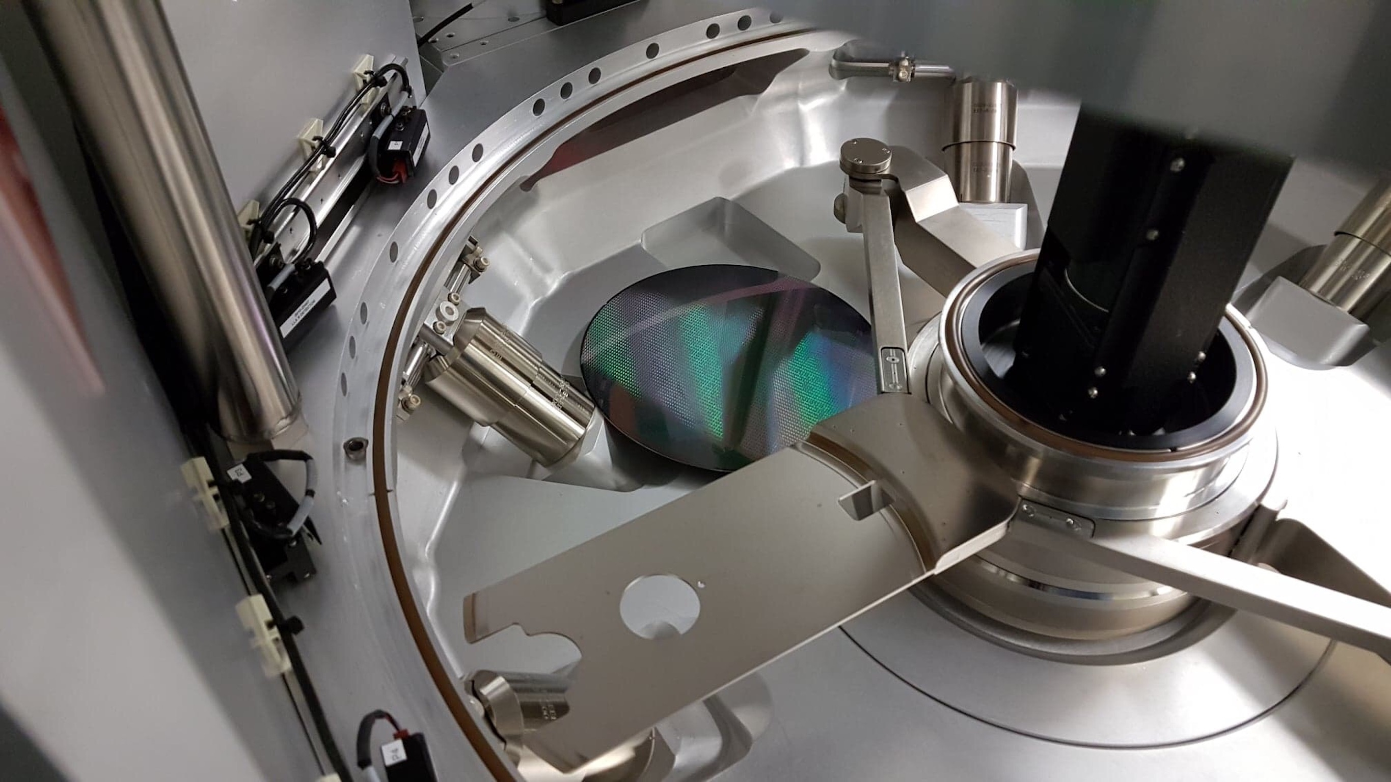
Vacuum Chamber
Unmasking the Extreme Tech Behind Miniaturized IC Chips
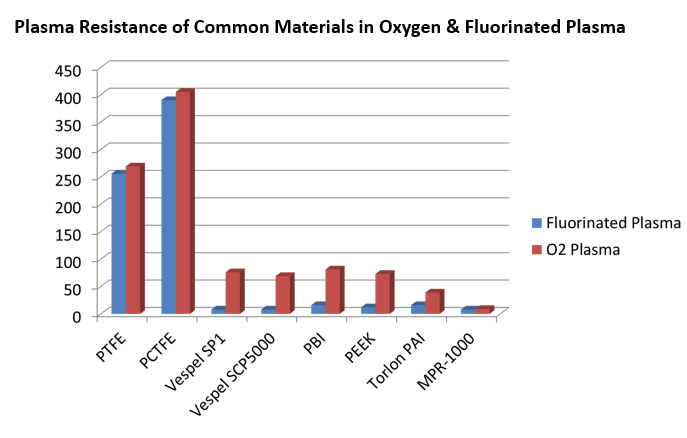
In manufacturing an IC chip several process tools are used to build the precise transistors at an atomic level. To be precise, at such minute levels requires processing often under vacuum pressure, within very aggressive plasma rich environments, at elevated heats, and under atomic level ionic purity requirements. For example, Dry etch process tools are used to remove a masked area to create trenches to build the transistors in. A typical trench is approximately 0.03 µm in length or 30 nm. Within the trench, 100s of transistors are built using ion implant and CVD process tools. Just one 45nm chip can contain 800,000,000 transistors. Critical to the manufacture of the chip is yield, which refers to the percentage of transistors that function properly. Thus, any plastics used within the chamber must not adversely affect the processing of the wafer.
Vacuum Chamber Process Tools
- Etch
- CVD (Chemical Vapor Deposition)
- Atomic Layer Deposition
- Ion Implant
Typical Applications
- Clamp Rings
- Shadow Rings
- Wafer Mobility applications
- Pins & Screws
- Seals and Insulators
Significant Properties
- Plasma Resistance
- Thermal Properties
- Ionic Purity
Typical Materials Families
- PEEK
- PEI – Ultem
- PAI – Torlon
- PBI – Celazole
- PI – Polyimide
- Fluoropolymers – (PTFE…)