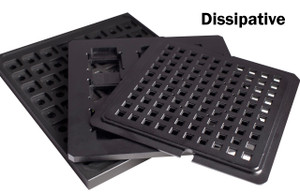
Semitron® CMP XL20, presented by Port Plastics and Mitsubishi Chemical Advanced Materials, represents the next generation in Chemical Mechanical Planarization (CMP) technology. Developed to enhance the efficiency of wafer production, this premium CMP material significantly increases the number of devices produced per wafer while simultaneously decreasing the cost of consumables per device. Achieved by extending the service life of the retaining ring, Semitron® CMP XL20 stands out for its high strength, stiffness, and superior uniformity, reducing edge defects and improving the overall quality of semiconductor wafers.
- INCREASED EFFICIENCY: Semitron® CMP XL20 enables more devices per wafer, significantly reducing consumables cost through extended service life.
- EXCEPTIONAL DURABILITY: Outperforms PPS up to 20x in most CMP processes, offering unparalleled durability and cost-effectiveness in semiconductor manufacturing.
- HIGH STRENGTH AND STIFFNESS: Promotes fewer edge defects and better wafer uniformity, crucial for high-quality semiconductor production.
- CHARCOAL/BLACK COLOR: Its distinctive color and opacity are designed for precision applications in semiconductor processes.
- COST SAVINGS: Lowers the overall cost per wafer, making semiconductor manufacturing more economical without compromising quality.
- COMPATIBLE WITH ADVANCED PROCESSES: Specifically developed for new tool designers and innovative end users focusing on future CMP technologies.
This innovative material outperforms PPS up to 20 times in most CMP processes, providing a significantly lower cost per wafer and marking a significant advancement in semiconductor manufacturing technologies. With its charcoal/black color and opaque finish, Semitron® CMP XL20 is designed for precision and efficiency, offering new tool designers and forward-thinking end users an invaluable resource for pushing the boundaries of what's possible in semiconductor production.


